- 您现在的位置:买卖IC网 > Sheet目录342 > MCB11C14 (Keil)BOARD EVAL FOR NXP LPC11C14
�� �
�
�NXP� Semiconductors�
�LPC11C12/C14�
�[15]� Allowed� as� long� as� the� current� limit� does� not� exceed� the� maximum� current� allowed� by� the� device.�
�[16]� To� V� SS� .�
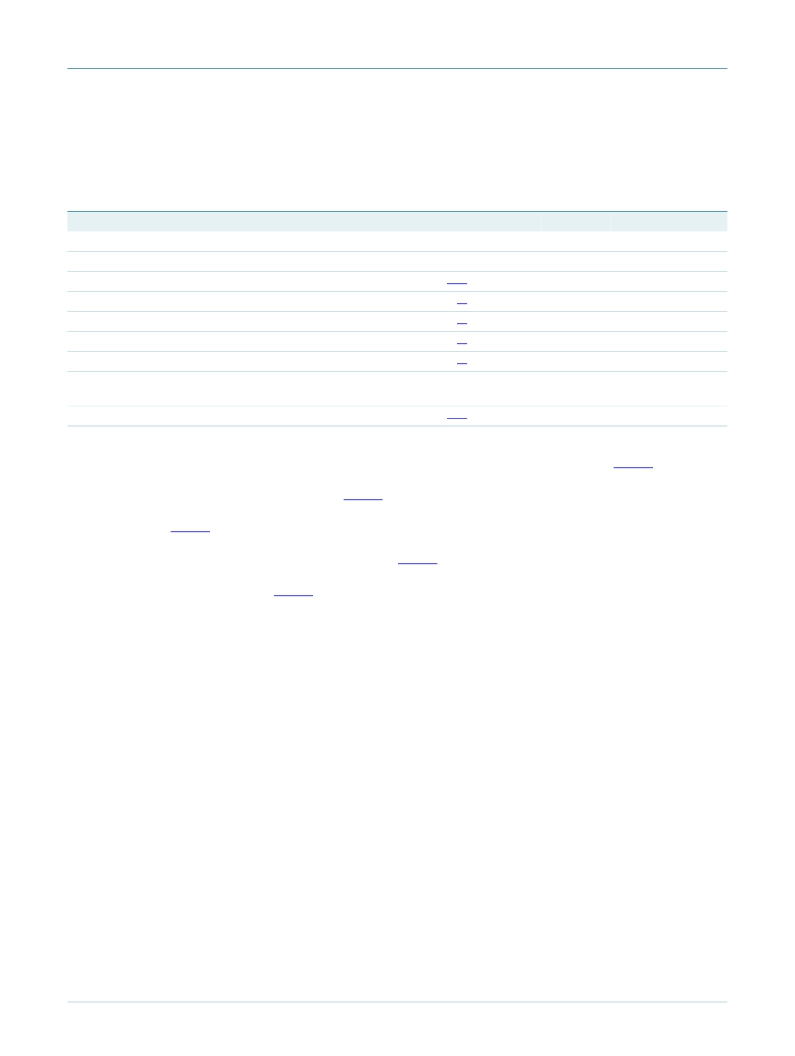
�Table� 6.� ADC� static� characteristics�
�T� amb� =� ?� 40� °� C� to� +85� °� C� unless� otherwise� specified;� ADC� frequency� 4.5� MHz,� V� DD� =� 2.5� V� to� 3.6� V.�
�Symbol�
�V� IA�
�C� ia�
�E� D�
�E� L(adj)�
�E� O�
�E� G�
�E� T�
�R� vsi�
�Parameter�
�analog� input� voltage�
�analog� input� capacitance�
�differential� linearity� error�
�integral� non-linearity�
�offset� error�
�gain� error�
�absolute� error�
�voltage� source� interface�
�Conditions�
�[1][2]�
�[3]�
�[4]�
�[5]�
�[6]�
�Min�
�0�
�-�
�-�
�-�
�-�
�-�
�-�
�-�
�Typ�
�-�
�-�
�-�
�-�
�-�
�-�
�-�
�-�
�Max�
�V� DD�
�1�
�±� 1�
�±� 1.5�
�±� 3.5�
�0.6�
�±� 4�
�40�
�Unit�
�V�
�pF�
�LSB�
�LSB�
�LSB�
�%�
�LSB�
�k� Ω�
�resistance�
�R� i�
�input� resistance�
�[7][8]�
�-�
�-�
�2.5�
�M� Ω�
�[1]�
�[2]�
�[3]�
�[4]�
�[5]�
�[6]�
�[7]�
�[8]�
�The� ADC� is� monotonic,� there� are� no� missing� codes.�
�The� differential� linearity� error� (E� D� )� is� the� difference� between� the� actual� step� width� and� the� ideal� step� width.� See� Figure� 5� .�
�The� integral� non-linearity� (E� L(adj)� )� is� the� peak� difference� between� the� center� of� the� steps� of� the� actual� and� the� ideal� transfer� curve� after�
��The� offset� error� (E� O� )� is� the� absolute� difference� between� the� straight� line� which� fits� the� actual� curve� and� the� straight� line� which� fits� the�
��The� gain� error� (E� G� )� is� the� relative� difference� in� percent� between� the� straight� line� fitting� the� actual� transfer� curve� after� removing� offset�
��The� absolute� error� (E� T� )� is� the� maximum� difference� between� the� center� of� the� steps� of� the� actual� transfer� curve� of� the� non-calibrated�
��T� amb� =� 25� °� C;� maximum� sampling� frequency� f� s� =� 4.5� MHz� and� analog� input� capacitance� C� ia� =� 1� pF.�
�Input� resistance� R� i� depends� on� the� sampling� frequency� fs:� R� i� =� 1� /� (f� s� � C� ia� ).�
�LPC11C12_C14_0�
�Preliminary� data� sheet�
�All� information� provided� in� this� document� is� subject� to� legal� disclaimers.�
�Rev.� 00.05� —� 23� April� 2010�
�?� NXP� B.V.� 2010.� All� rights� reserved.�
�25� of� 49�
�发布紧急采购,3分钟左右您将得到回复。
相关PDF资料
MCB2470
BOARD EVAL NXP LPC247X SERIES
MCBSTM32EXL
BOARD EVALUATION FOR STM32F103ZE
MCBTMPM330
BOARD EVAL TOSHIBA TMPM330 SER
MCIMX25WPDKJ
KIT DEVELOPMENT WINCE IMX25
MCIMX53-START-R
KIT DEVELOPMENT I.MX53
MCM69C432TQ20
IC CAM 1MB 50MHZ 100LQFP
MCP1401T-E/OT
IC MOSFET DRVR INV 500MA SOT23-5
MCP1403T-E/MF
IC MOSFET DRIVER 4.5A DUAL 8DFN
相关代理商/技术参数
MCB11C14-ED
制造商:ARM Ltd 功能描述:KEIL NXP LPC11C14 EVAL BOARD
MCB11C14U
功能描述:开发板和工具包 - ARM EVAL BOARD FOR NXP LPC11C14 + ULINK2
RoHS:否 制造商:Arduino 产品:Development Boards 工具用于评估:ATSAM3X8EA-AU 核心:ARM Cortex M3 接口类型:DAC, ICSP, JTAG, UART, USB 工作电源电压:3.3 V
MCB11C14UME
功能描述:开发板和工具包 - ARM EVAL BOARD FOR NXP LPC11C14 + ULINK-ME
RoHS:否 制造商:Arduino 产品:Development Boards 工具用于评估:ATSAM3X8EA-AU 核心:ARM Cortex M3 接口类型:DAC, ICSP, JTAG, UART, USB 工作电源电压:3.3 V
MCB11C14UME-ED
制造商:ARM Ltd 功能描述:KEIL NXP LPC11C14 EVAL BOARD
MCB11U10
功能描述:开发板和工具包 - ARM EVAL BOARD FOR NXP LPC11U14
RoHS:否 制造商:Arduino 产品:Development Boards 工具用于评估:ATSAM3X8EA-AU 核心:ARM Cortex M3 接口类型:DAC, ICSP, JTAG, UART, USB 工作电源电压:3.3 V
MCB11U10U
功能描述:开发板和工具包 - ARM EVAL BOARD FOR NXP LPC11U14 + ULINK2
RoHS:否 制造商:Arduino 产品:Development Boards 工具用于评估:ATSAM3X8EA-AU 核心:ARM Cortex M3 接口类型:DAC, ICSP, JTAG, UART, USB 工作电源电压:3.3 V
MCB11U10U-ED
制造商:ARM Ltd 功能描述:KEIL NXP LPC11U10 EVAL BOARD
MCB11U10UME
功能描述:开发板和工具包 - ARM EVAL BOARD FOR NXP LPC11U14 + ULINK-ME
RoHS:否 制造商:Arduino 产品:Development Boards 工具用于评估:ATSAM3X8EA-AU 核心:ARM Cortex M3 接口类型:DAC, ICSP, JTAG, UART, USB 工作电源电压:3.3 V